When a nuke goes off at the Alt D0
This board turned out to be un-repairable because of damage to the MCPx, but none the less it is an interesting read and has some wonderful pictures. I don't often write up repairs anymore, because they are all some variation of those already on this site. Not this time. This is something new. I pushed my soldering skills near their limit and learned a couple new things, even if I did fail to put another notch on my belt for fixing the un-fixable.
| So here is what I got when I opened the box | |
| This shot shows the retainer ring near the LPC. Commonly used as a ground point, the amount of solder present instantly made me wonder just how much heat this board was subjected to, and for how long. |
 |
| The top D0 looks to be in good shape. That's
always a promising sign :) A close visual inspection of the top D0 indicated that it was good and could be used for repairs if needed. |
 |
| Sacre Bleu! Holy Shit!, Good God, pick your favorite
explicative expression. All in all it looks like a Nuke was shot off while under the bottom D0 pad. |
 |
| Here is a wide view, We will dissect it here: In a nutshell, 4 of the traces (A0, A3, D0, D1) are torn away, the VIAs are in such bad shape (or missing) as to make soldering to them impossible. The blob of solder in the middle of the crater (clearly visible in the above picture, is doing a fine job of shorting out the 3.3 volt power plane to some or all of these signals, plus anything else in the area. After I calmed down from the laughter, I sent an e-mail asking just what had happened to this board. The replay? A temper tantrum. Hey, at least he's honest ;) |
 |
| Finally, we have some impact damage sustained during shipping. While this may not look like much, it actually indicates a fairly severe impact. Note, that the source of the impact was a hard drive (which appears to not have survived). |
 |
| After the initial photo essay of the board
and the damage (this is done for all boards by the way), it was time to
clean things up a bit and really assess how bad it was, and viability
for repair. I knew this one was going to be a challenge, and
likely not repairable, but I decided to dive in because the worst that
would happen is I'd get a bit of soldering practice in ;) While I have no direct photos after cleanup (they'd look about as good as the above pictures, but with less material on the boards, let me tell you, I did remove quite a bit of garbage from the "pit of despair" located at the former home of the Alt-D0 |
|
| Moving ahead to the repair portion, It became rather clear that there was no way to reliably solder to the vias on the back side of the board, which meant I'd have to use all the top side VIAs. This, in its self is not a problem; the TSOP on the other hand, is. | |
| Here we have the topside VIAs, as you can see some of the wires are soldered to the traces, while others were pressed into the via then soldered (this is the preferred method, as solder mask and VIA condition allow, two were too badly damaged on the back side to get the wire through. |
 |
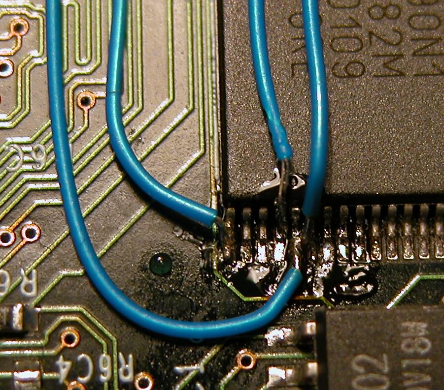
| This picture shows the close-up of the soldering to the
TSOP. This was not easy, and I am quite proud of the job I did on
it. The pins involved are 21, 24, 25, & 26; corresponding to A3,
A0, D0, & D1 respectively. It is no small task to solder leads
this size so close to each other, and I did this without a microscope,
as mine is currently out of commission :( Another thing to note is that while pin 25 and 26 look to be shorted, that is an artifact of the viewing angle, and in any case would not prevent booting from the LPC header. |
 |
| Here is a nice full view of the repair area. Notice the wires are kept similar length and as short as possible. It really scares me when people use half a foot of wire where an inch will do. The longer the wire, the greater the impedance mismatch, and the more noise you will pickup in your signal. Noise is bad. Too much noise and the part won't be able to tell a 1 from a 0. Also, the longer the wire the higher the inductance. The higher the inductance, the more retarded the rising and falling edges of your signal are. This impacts specifications such as setup and hold timings as well as jitter and overall signal integrity. [/rant] |
 |
| Alright, so in addition to the massive damage to the TSOP signals, pin 1 of the LPC was damaged as well. Here is a quick topside jump (bottom was too bad off for me to want to solder to it). |
 |
| And finally a close-up of the damaged area after removal of the surplus material and lake of solder. |
 |
| All content on this site is copyright 2006 networkBoy research. Permission to copy is hereby granted, with the express limitation that you need to link back here as attribution, and use in a commercial work requires my permission (royalties/licensing fees are negotiable) |  |